The Molecular Beam Epitaxy Lab (MBE), located in the Iowa Advanced Technology Labs (IATL), is part of the new Iowa Center for Research, Exploration, and Advanced Technology in Engineering and Sciences (Iowa CREATES), and managed by the Department of Physics and Astronomy.
About
What is molecular beam epitaxy?
- Ultrahigh vacuum technique for deposition of high purity epitaxial layers with high uniformity, atomic layer precision thickness control, and abrupt interfaces.
- Invented in the 1970s, a flexible and continually evolving technology for an increasing array of materials.
- A complementary technique to metal organic vapor phase epitaxy (MOVPE) for basic research, development, and commercial growth of semiconductor heterostructures.
Semiconductor crystalline layers are grown with single atomic layer precision from a handful of atomic layers thick to many microns with purities better than one part in ten billion. Epitaxy also allows layering different lattice-matched or strained semiconductors. See this presentation for more information.
Capabilities
- Growth of Group III-V compound semiconductors such as GaAs, GaSb, InAs, AlAs, AlSb, and related alloys
- Ga(Al)InAsSb bulk alloys and quantum wells
- Growth of strained layer In(Ga)As//InAsSb/GaSb superlattices and Ga(Al)InAsSb alloys.broken gap superlattices (e.g. InAs/GaSb, InAs/InAsSb)
- Growth and fabrication of core-shell nanowire heterostructures
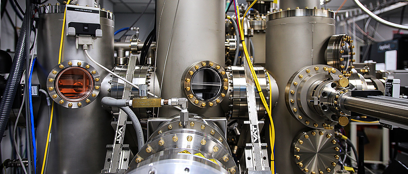
Growth Equipment
The facility consists of two carefully maintained, state-of-the-art growth chambers:
- Veeco EPI930 for growth on up 3” wafers
- A Gen20 for growth on up to 4” wafers
- Growth materials include Ga, Al, In, As, Sb, and dopants Te and Be
An ISO Class 5 clean room space is used for wafer handling and loading into the MBEs. Liquid nitrogen is delivered to both systems via a dedicated 6,000-gallon liquid nitrogen tank.
Growth Specific Characterization Equipment
- Spectrally resolved photoluminescence and electroluminescence
- High resolution X-ray diffraction
- Hall measurement
- Diode L-I and I-V characteristics
Applications
- LEDs (e.g. solid state lighting, consumer electronics, thermal scene generation)
- Diode lasers (e.g. optical communications and data storage, industrial welding and cutting, spectroscopy sensing of molecules, pumping solid state lasers)
- Photodiode detectors (e.g. consumer electronics, thermal cameras)
- High-electron-mobility transistors (HEMT) (e.g. used in cell phones)
- Photovoltaics (e.g. high efficiency solar cells, thermophotovoltaics)
Clients
- University of Iowa researchers
- Startup companies
- External users
Rates
(internal, 2023; external x 1.5)
- $225 per hour for epaxial growth of semiconductor heterostructures on MBE Growth Equipment
- $340 per hour external rate
- $40 per hour for characterization of MBE samples with Growth Specific Characterization Equipment
For more information, see this document.
Contact Us
If you are interested in growing or having III-V semiconductor heterostructures grown, please contact:
MBE Lab
IATL E121/151/151A
mbe-requests@uiowa.edu
319-335-3347